Saturday, December 31, 2011

Alarm Control System


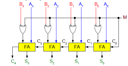
We wish to construct an alarm circuit such that the output remains active (on) even after the sensor output that triggered the alarm goes off(typical car alarm is representative of this type of circuit).The circuit requires a memory element to remember that the alarm has to be active until a reset signal arrives.
Such shown below of diagram of Alarm Control System Circuits


Some Important Videos About DLD 2


Some Important Videos About DLD 1


Wednesday, November 16, 2011

Binary Multiplier


Multiplication of binary numbers is performed in the same way as with decimal numbers.

The multiplicand is multiplied by each bit of the multiplier, starting from the least significant bit. 

The result of each such multiplication forms a partial product. Successive partial products are shifted one bit to the left.
The product is obtained by adding these shifted partial products.

Consider an example of multiplication of two numbers, say A and B (2 bits each), C = A x B.
The first partial product is formed by multiplying the B1B0 by A0. The multiplication of two bits such as A0 and B0 produces a 1 if both bits are 1; otherwise it produces a 0 like an AND operation. So the partial products can be implemented with AND gates.

BCD Adder


If two BCD digits are added then their sum result will not always be in BCD.
Consider the two given examples.


Binary Parallel Adder/Subtractor


The addition and subtraction operations can be done using an Adder-Subtractor circuit. The figure shows the logic diagram of a 4-bit Adder-Subtractor circuit.


The circuit has a mode control signal M which determines if the circuit is to operate as an adder or a subtractor

Carry Look Ahead Adder


In ripple carry adders, the carry propagation time is the major speed limiting factor.


Most other arithmetic operations, e.g. multiplication and division are implemented using several add/subtract steps. Thus, improving the speed of addition will improve the speed of all other arithmetic operations.

Tuesday, September 6, 2011

Implementation of a Full Adder with Decorder

Previously we have discussed about multiplexer circuit, decorder, encoder, half adder, full adder, half subtractor, full subtractor and universal gate. Now let we try to discuss about something else. So in this topic we will try to discuss about Combinational Logic Implementation. To write more specifically we will discuss about the implementation of a full adder circuit with a decorder and two OR Gates.

To do this at first we need to review the truth table of Full Adder circuit.

                                  Inputs
       a                            b                              c
              Outputs
         C              S

       0                            0                             0
          0              0
       0                            0                             1
          0              1
       0                            1                             0
          0              1
       0                            1                             1
          1              0
       1                            0                             0
          0              1
       1                            0                             1
          1              0
       1                            1                             0
          1              0
       1                            1                             1
          1              1
Fig: Truth table of Full Adder Circuit
From the truth table we have been found that
S(a,b,c)=sum(1,2,4,7)
C(a,b,c)=sum(3,5,6,7)

Wednesday, August 31, 2011

Multiplexers


Multiplexing means transmitting a large number of information units over a smaller number of channels or lines. A digital multiplexer is a combinational circuit that selects binary information from one of many input lines and directs it to a single output line. The selection of a particular input line is controlled by a set of selection lines. Actually there are 2^n input lines and n selection lines whose bit combinations determine which input is selected.

As an example we will discuss about a 4-line to 1-line multiplexer. Each of the four input lines, I0 to I3 is applied to one input of an AND Gate. Selection lines S1 and S0 are decoded to select a particular AND Gate. The truth table (shown below) lists the input to output path for each possible bit combination of selection lines. To explain the circuit operation let us consider the condition when S1S0=10. The AND Gate associated with input I2 has two of its inputs equal to 1 and the third input connected to I2. The other three AND Gates have at least one input equal to 0, which makes their output equal to 0. The OR Gate output is now equal to the value to the value of I2. A multiplexer is also known as a data selector, as it selects one of many inputs and steers the binary information to the output line.


Sunday, August 28, 2011

Encoder Circuit


An encoder is a digital function that produces a reverse operation from that of a decorder. The main difference between a decorder and an encoder is that a decorder has n number of input and 2^n number of output lines or channels. On the other hand an encoder has 2^n number of inputs lines and n number of outputs lines or channels. As example we can say about octal to binary encoder which consists of eight inputs and three outputs lines or channels. It is simply constructed with OR gate whose inputs can be determined from the truth table. The low order output Y0 is 1 if the input octal digit is odd. Output Y1 is 1 for octal digits 2, 3, 6 and 7. Output  is 1 for octal digits 2, 3, 6 and 7. Output Y2 is a 1 for octal digits 4, 5, 6 or 7. It is seen that input I0 is not connected to any OR gate, the binary output must be all 0’s in this case. All the 0’s output is also obtained when all inputs are all 0’s.

Friday, August 26, 2011

Decorder


In digital communication system there is a common name (decorder and encoder) to transfer data to desire position. In digital electronics we use decorder and encoder for this purpose. To simply speaking we use encoder to collect data of from a large number of channels or lines and transmitted as a few number of channels or lines. On the other hand we use decorder to collect the data that is transmitted by the encoder by a few number of channel or line and then distributed it to greater number of channels or lines (as required by the authority).


Discrete quantities of information are represented in digital system with binary codes.A binary code of n bits is capable of representing up to 2^n distinct elements of the coded information.A decorder is a combinatinal circuit that converts binary information from n inputs lines or channels to a maximum of 2^n unique lines.If the n-bit decoded information has unused or don’t-care combinations, the decorder output will have less than 2^n outputs.

Now we will try to construct a 3 to 8 line decorder. As mentioned earlier that, if a decorder has 3 input lines, it can handle data up to 2^3 or 8 output lines. Let we represent inputs as A0, A1 and A2 and outputs as D0, D1, D2, D3, D4, D5, D6 and D7.

Truth Table


     Inputs
   A0   A1     A2 
    Outputs
D0 D1 D2 D3 D4 D5 D6 D7    

    0      0       0    
1   0  0   0   0  0  0   0
    0      0       1
0   1  0   0   0  0  0   0
    0      1       0
0   0  1   0   0  0  0   0
    0      1       1
0   0  0   1   0  0  0   0
    1      0       0
0   0  0   0   1  0  0   0
    1      0       1
0   0  0   0   0  1  0   0
    1      1       0
0   0  0   0   0  0  1   0
    1      1       1
0   0  0   0   0  0  0   1


Thursday, August 25, 2011

Full Subtractor Circuit


The subtraction of two binary numbers may be accomplished by taking the complement of the subtrahend and adding it to the minuhend. By this method, the subtraction operation becomes an addition operation requiring full adders for its machine implementation. It is possible to implement subtraction with logic circuits in a direct manner. By this method, each subtrahend bit of the number is subtracted from its corresponding significant minuhend bit to form a different bit. If the minuhend bit is smaller than the subtrahend bit, a 1 is borrowed from the next significant position. The fact that a 1 has been borrowed must be conveyed to the next higher pair of bits by means of a binary signal coming out (output) of a given stage and going into (input) the next higher stage. It is same for the half-adder and full-adder, half-subtractor and full-subtractor circuits.

Half-Subtractor Circuit


Summery

The subtraction of two binary numbers may be accomplished by taking the complement of the subtrahend and adding it to the minuhend. By this method, the subtraction operation becomes an addition operation requiring full adders for its machine implementation. It is possible to implement subtraction with logic circuits in a direct manner. By this method, each subtrahend bit of the number is subtracted from its corresponding significant minuhend bit to form a different bit. If the minuhend bit is smaller than the subtrahend bit, a 1 is borrowed from the next significant position. The fact that a 1 has been borrowed must be conveyed to the next higher pair of bits by means of a binary signal coming out (output) of a given stage and going into (input) the next higher stage. It is same for the half-adder and full -adder, half-subtractor and full-subtractor circuits.

Tuesday, August 16, 2011

Full Adder Circuit


A Full Adder is a combinational circuit that performs the arithmetic sum of three input bits. It consists of three inputs and two outputs. Three of the input variables can be defined as A, B, Cin and the two output variables can be defined as S, Cout. The two input variables that we defined earlier A and B represents the two significant bits to be added. The third input Cin represents the carry bit. We have to use two digits because the arithmetic sum of the three binary digits needs two digits. The two outputs represents S for sum and Cout for carry.

For designing a full adder circuit, two half adder circuits and an OR gate is required. It is the simplest way to design a full adder circuit. For this two XOR gates, two AND gates, one OR gate is required. 

Half Adder Circuit


Half adder circuit is essential circuit for computer hardware components. The device which can calculate some integer or floating point wants half adder circuit. It is used for performing mathematical calculation in hardware. In computer, calculator and other counting device use half adder. It is the great invention for the scientists to sum the numbers easily. It consists of a XOR gate and two input pin and output sum and carry. Numbers of n bit are connected serially to add numbers.


Truth Table 

        Input A
        Input B
        Output C
        Output S
          0
           0
            0
           0
          0
           1
            0
           1
          1
           0
            0
           1
          1
           1
            1
           0

Thursday, July 21, 2011

Universal Gate NAND


Summery
In digital logic design we have familiar with various gate. Among these gates some are known as Universal Gate, some are well known as Basic Gates. In this topic we will try to discuss about the verification of Universal Gates, implementation of different logic gates with NAND gate. At last we will try to verify the truth table of different logic gates with NAND implementation.

Apparatus

Sl No
Name of the apparatus
 Rating
 Quantity
 1
 Dc Power Supply
 +5V dc
    1
 2
 IC(Quad-2 Input NAND Gate) HD74LS00P
 Vcc=5v,Vin=50
    2
 3
 Light Emitting Diode
 (1.5-3)v,(20-50)ma
    1
 4

Bread Board

    1
  5
Connecting Wire

   As required